

Abstract
Chemical transformation of existing two-dimensional (2D) materials can be crucial in further expanding the 2D crystal palette required to realize various functional heterostructures. In this work, we demonstrate a 2D 'on-stack' chemical conversion of single-layer crystalline MoS2 into MoO3 with a precise layer control that enables truly 2D MoO3 and MoO3/MoS2 heterostructures. To minimize perturbation of the 2D morphology, a nonthermal oxidation using O2 plasma was employed. The early stage of the reaction was characterized by a defect-induced Raman peak, drastic quenching of photoluminescence (PL) signals and sub-nm protrusions in atomic force microscopy images. As the reaction proceeded from the uppermost layer to the buried layers, PL and optical second harmonic generation signals showed characteristic modulations revealing a layer-by-layer conversion. The plasma-generated 2D oxides, confirmed as MoO3 by x-ray photoelectron spectroscopy, were found to be amorphous but extremely flat with a surface roughness of 0.18 nm, comparable to that of 1L MoS2. The rate of oxidation quantified by Raman spectroscopy decreased very rapidly for buried sulfide layers due to protection by the surface 2D oxides, exhibiting a pseudo-self-limiting behavior. As exemplified in this work, various on-stack chemical transformations can be applied to other 2D materials in forming otherwise unobtainable materials and complex heterostructures, thus expanding the palette of 2D material building blocks.
Export citation and abstract BibTeX RIS
Since the first mechanical exfoliation of two-dimensional (2D) crystalline graphene [1, 2], various dielectric and semiconducting analogues represented by h-BN and MoS2 have been isolated, revealing many new scientific phenomena and principles [3–9]. Despite being incompatible with mass production of large area samples, this simple exfoliation method can be applied to essentially any layered material with weak interlayer interactions [3], remaining one of the best methods for high quality crystals [10, 11]. Since most single layer (1L) transition metal dichalcogenides (MX2, where M and X denote the metal and chalcogen, respectively) are predicted to be thermodynamically stable [12], the palette of 2D crystals can be filled with tens of metallic, semiconducting and insulating 'colors'. In contrast to 'top-down' exfoliation, it was also shown that 2D crystals and their heterostructures can be constructed 'bottom-up' from appropriate building blocks via chemical routes as demonstrated by the vapor deposition of graphene and other crystals [13–17]. Alternatively, arbitrarily stacked extended 2D structures can be formed by physically stacking one 2D crystal on top of another, exploiting interplanar van der Waals (vdW) interactions [18]. Even with limited 'colors' available, there have already been interesting 2D heterostructure-related reports, such as tunable metal–insulator transitions [19], field effect tunneling transistors [20], and photodetectors [21].
Chemical transformation of existing 2D materials may also be useful in further expanding the 2D crystal palette required to realize various functional heterostructures. The top single, few or even all layers of supported 2D materials may be selectively transformed into another of a different chemical nature by choosing appropriate chemical reactions. Such 'on-stack transformations' may form 2D materials that are not readily generated via conventional synthetic routes or physical vdW stacking routes. This presents a challenge and opportunity for chemists and materials scientists to explore and develop various chemical reactions that can be applied to each type of 2D crystal. Considering the high aspect ratio (length-to-thickness) of 2D materials, precise control over the thickness of modified layers further requires a given reaction to be highly uniform across the basal planes. In addition, chemical reactions of 2D materials are also of fundamental significance and deserve systematic investigation since their unique geometric and electronic properties may lead to novel phenomena and findings characteristic of low dimensional materials. For example, the chemical reactivity of 1L graphene was shown to be much higher than few layer-thick graphene for facile out-of-plane distortion [22–24] or larger susceptibility towards external charge doping [25]. Even the edges of graphene are distinct from the inner area in terms of chemical reactivity [24] and electronic properties [26]. The presence of solid substrates, atomically rough in most cases, has profound effects on the geometric [10, 11, 27] and electronic structures [28], chemical reactivity [23] and wettability [29] of the supported graphene.
In this regard, chemical transformation between chalcogenides of transition metals can be a model reaction to explore the chemistry of 2D materials. While the disulfides and diselenides of molybdenum have a strong tendency towards oxidation [30], the resulting trioxides may also be reduced to dichalcogenides in an excess of chalcogenic precursors at elevated temperatures [31, 32]. Atomically thin MoS2 has been well studied, drawing great interest for its direct-indirect bandgap transition [5, 7] depending on the number of layers, thus revealing rich photophysics [33] and allowing various optoelectronic applications [34]. MoO3, with a larger bandgap (>2.7 eV), is photochromic [35] and electrochromic [36], and has thus been actively investigated for its potential in displays and smart windows [37]. With a large work function of 6.7 eV, MoO3 films also serve as hole dopants as well as hole transport layers [38]. Due to its high dielectric constant, MoO3 may serve as an ideal gate dielectric [38] for atomically thin transistors based on 2D semiconductors [39]. Although there have been many studies on thin MoO3 films formed by thermal and sputter deposition [37], their surfaces exhibited a typical roughness larger than a few nm [40], far from the layer-by-layer precision that can be routinely achieved with various 2D crystals. Since atomically thin MoS2 layers of high crystallinity or large area can be prepared, respectively, by the exfoliation [3] or chemical vapor deposition (CVD) method [41], 2D oxides of atomic thickness may be generated by chemical transformation of the 2D sulfides.
In this work, we demonstrate O2-plasma-based conversion of 2D MoS2 crystals into highly flat 2D MoO3 or MoO3/MoS2 heterostructures with layer-by-layer precision. As the plasma oxidation time increased, the Raman and photoluminescence (PL) intensity from MoS2 decreased, indicating loss of the sulfides. X-ray photoelectron spectroscopy (XPS) showed that Mo6+ increased at the expense of Mo4+, confirming the conversion. Optical second-harmonic generation (SHG) spectroscopy revealed a drastic alteration in intensity, which is explained by the breakage and recreation of inversion symmetry in the remaining crystalline sulfides. The plasma-generated 2D oxides were highly flat, with a typical roughness of 0.18 nm. The thickness of a single layer oxide was 1.8 ± 0.1 nm, ∼2.5 times the interlayer spacing of crystalline α-MoO3. Systematic Raman and atomic force microscopy (AFM) measurements also revealed that the oxidation proceeded from the top layer into the underlying layers, with the rate decaying rapidly due to the passivation effect of the surface oxide layers. Our study suggests that similar on-stack chemical transformations can be devised to convert one form of 2D chalcogenide into another or their heterostructures, which should expand the palette of 2D materials.
Results and discussion
Raman spectroscopic characterization of 2D sulfides and their oxidation
Figures 1(a) and (b) show optical micrographs of 1L and 2L MoS2 (1LMS and 2LMS, respectively) obtained before and after a series of exposures to low-frequency O2 plasma (see methods for the details). The accumulated exposure time (tox) represents the total reaction time. The optical contrast of both samples significantly decreased at tox ≥ 26 s, and the flake of 1LMS could be barely identified at tox = 242 s. The change in the optical contrast was attributed to the conversion to 1L MoO3 (1LMO) with negligible absorption in the visible range, as will be shown below. A similar contrast change was observed for nLMS (n = 3–4) (see figure S1). Figure 1(c) shows the Raman spectra of 1LMS obtained in the ambient conditions at various tox. Among the four Raman-active modes of bulk 2H-MoS2 (space group  [42], the in-plane
  and out-of-plane
  were shown to be useful in determining the number (n) of layers of thin MoS2 samples [6]. Although their symmetry representations vary depending on n (E' and A1' for odd-numbered nLMS belonging to the
  space group; Eg and A1g for even-numbered nLMS belonging to the
  space group) [43], the bulk-notations will be used for simplicity according to the original report for 1L [6]. The frequency difference (Δω) of the two Raman peaks was found to be 18.5 cm−1, and their widths were comparable to those of the previous report [6], which confirms that the sample is single-layered. The lack of the defect-activated LA(M) peak also verifies its high structural quality (figure S2) [44]. As further direct evidence, atomically resolved transmission electron microscope (TEM) images and diffraction patterns were obtained for freestanding 1L samples (figure S3).
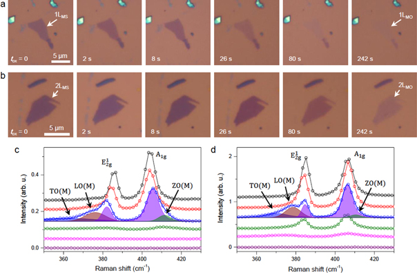
Figure 1. Raman spectroscopic characterization of plasma-oxidized MoS2. (a) and (b) Optical micrographs of single and double-layer MoS2 (1LMS and 2LMS) obtained after O2 plasma treatment for varying oxidation time (tox). When completely oxidized after 242 s, both samples became transparent, indicating formation of the corresponding 2D Mo oxides (1LMO and 2LMO). (c) and (d) Raman spectra of 1L and 2L MoS2, obtained with increasing tox of (top to bottom) 0, 2, 8, 26, 80 and 242 s. The raw spectra (open circles and solid lines) were offset for clarity. The blue solid lines for tox = 8 s are cumulative fits of five Voigt functions representing the color-shaded Raman peaks: two violets for  and
and  one blue peak for TO(M), one wine for LO(M) and one olive for ZO(M) (see the text for their assignment).
Download figure:
Standard image High-resolution imageOxidation induces a few distinctive changes in the Raman spectra. The in-plane Raman mode softened by ∼1 cm−1 on the first exposure for 2 s and downshifted further with the other mode moving in the opposite direction when subjected to additional exposure (tox = 8 s). Since the newly evolving Raman peaks have both lower and higher peak frequencies than their pristine counterparts, their frequency difference, Δω(NC), is ∼5 cm−1 larger than that of pristine 1LMS. Both peaks also broadened asymmetrically and displayed attenuated intensity. For tox = 26 s, when significant loss was observed in the optical contrast in figure 1(a), for example, the Raman intensities I( and I(A1g) decreased to ∼5% of those for the pristine sample, with both peaks moving further away from each other and further broadening. The additional exposure (tox = 80 s) led to no detectible signal for both peaks, indicating complete loss of MoS2. Within the phonon confinement model, the oxidation-induced downshift (upshift) of
  (A1g) can be explained by the relaxation of the fundamental Raman selection rule [45]. In essence, the defects confining phonons allow scattering of phonons with energies lower (higher) than
  (A1g) near the zone center. The low (high)-frequency shoulders of
  (A1g) that caused the asymmetric broadening are also due to the defects, which selectively allow scattering of the phonons near the M points in the double-resonance Raman scattering mechanism [46]. Indeed, the spectra of partially oxidized 1L and 2L (figures 1(c) and (d)) are well described by the five Voigt functions, including the defect-activated TO(M), LO(M) and ZO(M) [44, 45]. As discussed in detail below, plasma-generated reactive oxygen species create sub-oxide defects (MoSxO1−x) on the basal plane of MoS2, essentially forming a nanocrystalline (NC) phase MoS2 sheet.
The Raman spectra of multi-layered samples showed similar spectral changes with a layer-by-layer oxidation behavior. The in-plane mode of 2LMS in figure 1(d), for example, showed a noticeable broadening due to the M-point phonons for tox = 8 s and became sharper with 40% attenuated intensity for tox = 26 s. Additional exposure (tox = 80 s) led to a further decrease in intensity and significant broadening. The NC-phase observed for tox = 8 s is formed on the top MoS2 layer, with the bottom layer remaining intact. The disappearance of the NC-phase features for tox = 26 s can be attributed to complete oxidation of the top layer, which is only weakly coupled with the still pristine bottom layer responsible for the remaining half of the Raman signals. The second appearance of the broadening for tox = 80 s indicates that the oxidative attack reached the bottom layer, forming NC-phase domains. Additional exposure (tox = 242 s) led to a complete loss of Raman signal. These observations indicate that the oxidation proceeds in a layer-by-layer manner and is much slower for inner layers that are protected by the outer oxides.
Symmetry characterization by SHG
Since optical SHG requires a lack of inversion symmetry [47], it can serve as a sensitive symmetry probe for chemical modification occurring in thin MoS2. As shown in figure 2(a), a strong SHG signal occurred at 400 nm when the fundamental 800 nm Ti:sapphire laser beam with a nominal pulse width of 140 fs was irradiated on non-centrosymmetric pristine 1LMS [48]. An input power dependence of the SHG peak intensity (ISHG) confirmed the two-photon process (figure S4). The intensity of the SHG peak (ISHG) indeed decreased with the plasma oxidation and finally reached zero for 1LMO (tox = 20 s), which correlates nicely with the Raman intensity variation of MoS2 (figure 2(b)). Thus, the attenuation of ISHG can be attributed to the destruction of the 1L MoS2 crystal. As shown in figures 2(a), 2L MoS2 presents a striking contrast to the case of 1L. ISHG(2LMS) is ∼60 times smaller than ISHG(1LMS) because even-number-layered MoS2 crystals are centrosymmetric and thus do not support SHG. The residual signal of 2LMS is attributed to a minor interlayer asymmetry induced by the presence of the SiO2/Si substrate [49]. A series of oxidation treatments, however, activated and then deactivated SHG by the 2L flake (figure 2(a)). Figure 2(b) reveals that ISHG intensity increased at the expense of the Raman signal represented by I(A1g). Since ISHG reached its maximum at tox = 30 s, for which the Raman intensity is close to that of 1LMS, the treated sample essentially corresponds to 1LMO/1LMS. This assignment is also supported by the fact that additional treatments led to a decrease in ISHG, indicating oxidative degradation of the bottom sulfide layer. The lack of SHG signal from the completely oxidized layers (1LMO and 2LMO) might be explained if the 2D oxides are a centrosymmetric crystal such as bulk α-MoO3 and belong to the space group of  [50]. As will be shown below, however, the 2D oxides are far from α-MoO3 and more likely to be amorphous and isotropic, thereby not generating SHG signals.

Figure 2. Nonlinear optical characterization of plasma-oxidized MoS2. (a) Optical SHG spectra of 1L and 2L MoS2 obtained at increasing tox of (top to bottom) 0, 10, 20, 30, 40, 60, 80 and 240 s. (b) Raman and SHG intensities of 1L and 2L MoS2 given as a function of tox. The maximum intensity of 2L, at tox = 30 s, is ∼1/3 of that for the pristine 1L. (c) Schematic view (left) of the MoS2 lattice with armchair and zigzag edges and an optical image (right) of 1L MoS2 used in the SHG measurements. With the polarization directions of the input  and output
  fixed, the sample with a predefined laboratory axis
  was rotated by θ. The armchair direction
  forms an angle
  with respect to
  (d) Polar plot of the parallel SHG intensity
  of pristine (gray) and half-oxidized (magenta) 1L MoS2 given as a function of θ. Using the fact that
  which is represented by the solid lines, the armchair direction of the sample is determined with θ0 = 15.0° ± 0.2°.
Download figure:
Standard image High-resolution imageDespite the degradation of the crystalline lattice, the crystallographic orientation could still be determined for partially oxidized MoS2 since ISHG is strongly dependent on the polarization angle  between the fundamental polarization
  and armchair direction
  as defined in figure 2(c). For polarization-resolved SHG measurements, samples were rotated to vary θ, and the SHG signal parallel to the input polarization,
  was collected using a polarizer located in front of the detector. The polar plot for 1LMS in figure 2(d) revealed the 6-fold symmetry of
  [48], which also determined that θ0 = 15.0° ± 0.2°, the angle of
  with respect to a preset laboratory axis (
 When oxidized to give ∼0.4 LMS, as judged from its Raman spectra (tox = 15 s),
  decreased by ∼75% but still showed the same angular dependence as the pristine 1LMS. The oxidation-induced modulation in ISHG (figures 2(a) and (b)) and the robust θ-dependence demonstrate that the SHG process can be utilized to characterize chemical changes in 2D materials.
Formation of ultraflat 2D oxides with single-layer precision
The on-stack transformation was found to proceed in a layer-by-layer manner and could be controlled with a high thickness resolution, even allowing formation of single-layer MoO3. To monitor morphological changes from the transformation, an amplitude-modulated, non-contact AFM was exploited. The height profile across the pristine 2LMS-1LMS area in figure 3(a) revealed a step with a height of 0.70 ± 0.1 nm, which agrees well with the interlayer spacing (0.62 nm) of 2H-MoS2 [51]. Note that the height of the 1LMS-SiO2 step varied over 1.2–1.8 nm from sample to sample due to the chemical and electrostatic contrast between dissimilar materials [52, 53] and interlayer molecular species trapped during the exfoliation. When 2LMS was completely oxidized (tox = 242 s), the 2LMO-1LMO step height increased to 1.8 ± 0.1 nm (figures 3(b) and (e)). As depicted in figure 3(f), the step height corresponds to the thickness of single-layer MoO3 and is ∼2.5 times the interlayer spacing (0.69 nm) of α-MoO3 [50]. A similar change was observed for the 2LMS-1LMS step of another sample when treated for tox = 242 s (figures 3(c) and (d)). After the same treatment, however, the 3LMS-2LMS step height changed only by ∼0.2 nm. In contrast to the 2L region, the Raman spectrum of the 3L region showed that ∼15% of the lowermost layer remained intact (see figure S5 for Raman spectra obtained after each step of the sequential oxidations). Thus, the step height measured across the 3L-2L region corresponds to the thickness of the partially oxidized bottom layer.
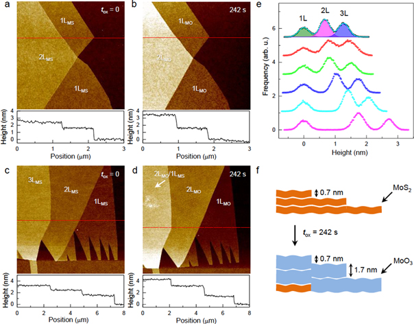
Figure 3. Layer-by-layer oxidation of few-layer MoS2. (a) and (b) Non-contact AFM height images of a 1LMS-2LMS sample obtained before and after oxidation (tox = 242 s). Height profiles across the red lines in (a) and (b) are also shown below the AFM images. (c) and (d) Non-contact AFM height images of another sample with 1LMS, 2LMS and 3LMS regions before and after oxidation (tox = 242 s). Height profiles across the red lines in (c) and (d) are also shown below the AFM images. (e) Height histograms of the sample in (c) and (d) obtained for the 1L, 2L and 3L areas as a function of tox at (top to bottom) 0, 2, 8, 26, 80 and 242 s. The mean height of 1L area was set to be zero. Root-mean-square roughness (Rq) of each area was determined by fitting the data with 3 color-shaded Gaussian functions as shown for the pristine sample (see figure S6 for the variation of the roughness induced by the oxidation). (f) Schematic diagram of 'top-down' layer-by-layer oxidation that converts MoS2 into MoO3.
Download figure:
Standard image High-resolution imageDespite the increase in thickness, MoO3 layers were still highly flat, as seen in the AFM height images in figure 3. The change in the surface morphology of the 2D oxides was further quantified by the root-mean-square roughness (Rq), or standard deviation of height distribution, shown in figure 3(e). The Rq of 1LMS was 170 ± 10 pm, which is slightly higher than that of graphene [54] and equivalent to that of completely oxidized 1LMO, 180 ± 10 pm for tox ≥ 80 s, as shown in figure S6. Notably, however, the surface roughness showed a spike of 230 ± 10 pm for tox = 2 s and a sharp decrease for tox = 8 s. Similar spikes were also observed for 2LMS and 3LMS when treated for 2 s. The Rq values of 2LMO and 3LMO (170 ± 10 pm) are also equivalent to those of their pristine counterparts. We attribute the roughness surge to clusters of partially oxidized MoS2, possibly molybdenum oxysulfides (MoSxOy) [55] that serve as nucleation sites during the plasma oxidation. This picture is also corroborated by the drastic PL quenching for tox = 2 s, as will be shown below. However, the Raman spectra did not show a noticeable change (figures 1(c) and (d)) because the majority of the sample remained intact for the short reaction time.
Chemical nature of 2D oxides
The chemical transformation was revealed by XPS. Because the probe size of the XPS instrument was larger than the typical size of the exfoliated samples (<20 μm), large-area MoS2 films grown by the CVD were used (see methods for the details of preparation). While the effective thickness was found to be 2L based on the peak difference (Δω), their Raman intensity was lower than that of mechanically exfoliated samples, suggesting lower crystallinity (figure S7). Figure 4(a) presents the Mo 3d spectra obtained as a function of tox. The pristine sample showed the strong doublet of Mo4+ arising from MoS2, with a binding energy (EB) of 229.5 eV (232.6 eV) for 3d5/2 (3d3/2), which is consistent with the average literature value of EB(3d5/2) = 229.25 eV for bulk MoS2 crystals [56]. The Mo6+ species of the pristine sample, responsible for the minor doublet with EB = 232.7 eV (235.7 eV) for 3d5/2 (3d3/2), were attributed to residual MoO3 (<20% of the total Mo species) formed before or after the CVD growth. Upon plasma treatment, the Mo6+ doublet grew significantly at the expense of the Mo4+ doublet, indicating the conversion to MoO3. The oxidation was also confirmed by the decrease in the intensities of the S 2 s peak (EB = 226.7 eV) in figure 4(a) and the S 2p doublet (EB = 161.9 eV for 2p3/2) in figure 4(b). The current data cannot exclude the possibility that a small fraction of Mo5+ species (EB = 231.1 eV for 3d5/2) [57], representing oxygen vacancy defects generated by incomplete oxidation, may be present.

Figure 4. Elemental analysis of plasma-oxidized MoS2. (a) Mo 3d XPS spectra of CVD-grown 2LMS samples oxidized for various tox of (top to bottom) 0, 2, 8, 26, 80 and 242 s. The spectra were fitted with multiple mixed Lorentzian–Gaussian functions. The green shades correspond to Mo4+ (3d5/2) and Mo4+ (3d3/2) peaks and the violet shades to Mo6+ (3d5/2) and Mo6+ (3d3/2) peaks. At the binding energy of ∼227 eV, the S 2 s peak can be observed. (b) S 2p XPS spectra of the same samples shown in (a). The spectra were also fitted with two sub-peaks, 2p1/2 and 2p3/2. (c) The overall photoelectron intensity of Mo species and atomic fractions of Mo4+ and Mo6+ given as a function of tox.
Download figure:
Standard image High-resolution imageTo shed more light on the chemical transformation, we obtained optical absorption spectra using reflectance spectroscopy (figure 5, see methods for the details). For a very thin film (thickness  λ) supported on a thick transparent substrate with a refractive index of n0, the fractional change in reflectance
  is given as follows:
  where R, R0 and A are the reflectance of the film, reflectance of the bare substrate, and absorbance [58]. Pristine 1LMS–3LMS exfoliated on quartz substrates showed characteristic absorption peaks at 1.90, 2.05 and 2.85 eV, which were denoted, respectively, by A, B and C as per an earlier work [59]. The two former excitonic peaks originate from the direct-gap transitions between the valence and conduction bands at the K points in the Brillouin zone [5]. The high energy peak, C, arises from nearly degenerate multiple excitonic states [60] or transitions across nested valence and conduction bands [61]. All three peaks downshifted in energy with increasing thickness [5]. When the samples were treated for tox = 80 s, which is expected to oxidize ∼1.7L, the overall absorbance decreased significantly for all thicknesses. The A and B peaks of 1L, in particular, almost disappeared, with the major absorption edges relocated to >2.7 eV, which agrees well with the fact that MoO3 is a wide-bandgap semiconductor [62]. The partially oxidized 2L exhibited downshifts of the A and B peaks but an upshift of the C peak, and 3L exhibited similar shifts but to a lesser degree. The spectral changes are attributed to the oxidation-induced defects and can be explained by the drastic changes in the electronic band structures of O-substituted MoS2 [63]. To determine the optical bandgap of the 2D MoO3, Tauc plot analysis was taken for the UV/Vis absorption spectra of CVD-grown large-area samples (figure S8). Despite some inconsistencies in the literature [64], it is generally accepted that an optical gap energy (Eg) of an amorphous semiconductor can be extrapolated using
  [65, 66], where α,
  and m are, respectively, the absorption coefficient, photon energy and an exponent specifying the nature of the optical transition (m = 2 for an indirect allowed transition; m = 1/2 for a direct allowed transition). By choosing m = 2 for α-MoO3 as an indirect bandgap semiconductor [67], Eg was determined to be ∼3.0 eV for 1LMO and 2LMO. The resulting bandgap energies are in a good agreement with those of α-MoO3 crystals [62] and thermally deposited MoO3 films [68, 69]. Despite the similar bandgap energies and apparent layered structure of plasma-generated MoO3, however, no Raman signal could be detected from the 2D oxides, possibly due to their amorphous nature. A careful Raman analysis in comparison with mechanically exfoliated thin α-MoO3 crystals set an upper bound for α-MoO3 content of ∼1% (figure S9).
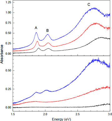
Figure 5. The absorption spectra of 1L–3L MoS2 exfoliated onto quartz substrates: (top) before and (bottom) after oxidation for tox = 80 s. The absorbance was determined from optical reflectance contrast measurements (see Methods for the details). See the text for the origins of the three prominent peaks denoted by A, B and C. For comparison with UV/Vis transmission measurements for CVD-grown samples and estimation of their optical bandgaps using Tauc plots, see figure S7.
Download figure:
Standard image High-resolution imagePL intensity modulation
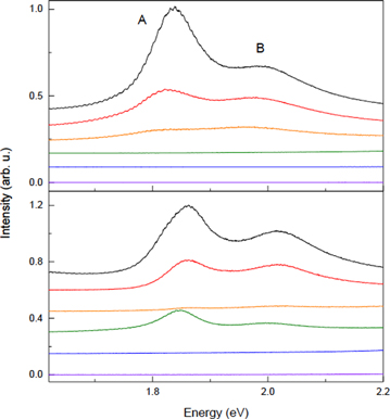
The change in the PL spectra in figure 6 revealed further details of the chemical modifications occurring in 2D MoS2. The PL spectrum of the pristine 1LMS mainly consists of the two exciton peaks A and B, respectively located at 1.84 and 2.00 eV, which is in good agreement with the absorption spectra. Both originate from the direct-gap transitions between the conduction and valence bands at the K points in the Brillouin zone [5, 7]. First, we note that the PL is drastically quenched by the plasma treatments. After a 2 s exposure, for example, the intensity of A (IA) decreased by ∼65%, although the Raman spectra in figure 1 show no significant change in I and I
and I The quenching can be attributed to the plasma-generated defects that were confirmed by the defect-induced Raman peaks, as will be further discussed below. When further defects were introduced to form the NC phase (tox = 8 s), the PL intensity was only ∼10% of the pristine value. The completely oxidized 1LMO gave no PL signal, which is consistent with the fact that its Eg is larger than the excitation photon energy of 2.41 eV. 2LMS in figure 6(b) shows a similar defect-mediated PL quenching—∼60% decrease for tox = 2 s and almost zero PL signal for tox = 8 s, which introduced a significant number of defects judging from the Raman spectrum (figure 1(c)). Upon further oxidation (tox = 26 s), however, the PL intensity increased back to ∼30% of that for the pristine 2LMS. We note that the Raman spectra showed that the top layer was almost completely oxidized with the bottom layer mostly intact (figure 1(d)). This suggests that the system essentially became a 1LMO/1LMS/SiO2 sandwich, which further corroborates the layer-by-layer oxidation. Thicker samples showed a similar trend, but the PL intensity oscillation of nLMS could be seen only when tox was selected in such a way that (n − 1)LMO/1LMS was nicely formed.
Figure 6. Photoluminescence spectra of 1L (top) and 2L (bottom) MoS2 for varying tox of (top to bottom) 0, 2, 8, 26, 80 and 242 s. The two emission peaks denoted by A and B have the same origins as the corresponding absorption peaks in figure 5.
Download figure:
Standard image High-resolution image
Structural defects in crystalline semiconductors have various modes of interaction with excited charge carriers, and their interactions become more significant in lower dimensional materials due to confined wave functions within a tighter space. For carbon nanotubes with low lying dark exciton states, sp3-type defects form new sets of radiative energy levels granting an enhanced PL quantum yield [70]. Defects may trap excited free charge carriers and mediate ultrafast Auger decay of photoexcitation in quantum dots [71]. Excitons can be localized at defects and radiatively decay at lower energies, as shown for 1L MoS2 irradiated with α particles [72] and 1L WS2 treated with Ar plasma [73]. Defects in some 2D semiconductors have also been shown to serve as single photon emitters [74, 75]. Localization followed by non-radiative decay is one among various quenching routes of excitons, which also include exciton-exciton annihilation and electron–phonon interactions [76]. The PL quenching observed at the very early stage of the oxidative conversion can be attributed to partially oxidized defects, including the nanometer scale protrusions that were responsible for the roughness spikes (figure S6). The higher defect-sensitivity of PL can be more clearly seen in the comparison between Raman and PL intensities given as a function of tox (figure S10).
Layer-by-layer conversion
The overall change can be summarized by the scheme for 3LMS with terraces of 2LMS and 1LMS presented in figure 3(f). At the early stage of reactions (tox = 2 s), the top surface of 3LMS exposed to the gaseous oxidants undergoes partial oxidation forming nanometer-scale oxysulfides (MoSxOy) clusters that are responsible for the increased Rq. At this stage, the average thickness of the top layer is not much different from that of pristine 1LMS or the interlayer spacing of 2H-MoS2 crystals. Although the Raman spectra reveal no significant change, the PL intensity of 3LMS drops significantly due to the defects serving as PL quenchers. Additional exposure to oxidants induces the NC-phase Raman peaks and almost complete quenching of the PL. When the first top layer is completely converted to MoO3, its thickness increases to 1.8 nm, which is 2.5 times the interlayer spacing of α-MoO3 crystals. At this stage where 1LMO/2LMS is formed, the PL intensity can be recovered back to that of 2LMS because of the lack of quenching sites within the remaining 2LMS. Further exposure will repeat the above reactions for the second top layer but with a greatly decreased reaction rate.
Although the Raman analysis suggests that the 2D oxides are amorphous, their high flatness and modulation in SHG and PL intensities indicate that the oxidation reaction proceeds in the layer-by-layer manner. Thus, it is likely that the oxides are also layered like α-MoO3. Since the number density of Mo in a single α-MoO3 layer [67] is 18% higher than that for 1LMS [51], a 2D conversion into the crystalline oxide would lead to a large tensile strain (∼9%) when the areal density of Mo is maintained or generate voids requiring significant mass transport to compensate for the difference in the Mo densities. Moreover, the average thickness of 1LMO (figure 3) is 2.5 times the interlayer spacing of α-MoO3. These facts suggest that the 2D oxides are much less dense than α-MoO3. Despite the apparent flatness and lack of pits or cracks in the 2D oxides, these considerations lead us to conclude that there must be numerous structural irregularities, including fine voids, that cannot be detected by the AFM probes. Our results also showed that the plasma oxidation is highly effective for the topmost sulfide layer and increasingly slower for the next buried layers. Such voids may serve as a route for the oxidants required for the reactions underneath the top layer.
In summary, we demonstrated a model 2D chemical reaction that converts 1L sulfides into 1L oxides, thus allowing MoO3/MoS2 heterostructures. Single and few-layer MoS2 prepared via micromechanical exfoliation of 2H-MoS2 crystals were treated with strong oxidants generated from O2 plasma. The early stage of the reaction was detected by defect-induced Raman peaks, drastic quenching of PL signals and sub-nm protrusions in AFM images. As the reaction proceeded from the uppermost layer to buried layers, PL and SHG signals showed characteristic modulations revealing a layer-by-layer conversion. The plasma-generated 2D oxides, confirmed as MoO3 by XPS, were found to be amorphous but highly flat with a surface roughness of 0.18 nm, comparable to that of 1L MoS2. The rate of oxidation quantified with Raman spectroscopy decreased very rapidly for buried sulfide layers due to protection by the surface 2D oxides. As exemplified in this work, the on-stack chemical transformation can be applied to other 2D materials in forming otherwise unobtainable materials and complex heterostructures, thereby expanding the palette of 2D material building blocks.
Experimental section
Mechanical exfoliation
Single and few-layer MoS2 samples were prepared by mechanical exfoliation [3] of molybdenite, a natural mineral of 2H-MoS2 (SPI). Silicon wafers with 285 nm thick SiO2 layers were used as substrates. Ultrathin layers of MoS2 were identified using an optical microscope, and their numbers of layers and quality were determined using Raman spectroscopy [6]. To prepare thin α-MoO3 crystalline flakes as a Raman standard (figure S9), a similar mechanical exfoliation was applied to a powder of MoO3 (Materion).
Growth of large-area samples by CVD
Two different CVD growth methods were used in synthesizing large area MoS2 films. In one approach for the samples used for XPS measurements, Mo metal of 0.5 nm for 2LMS was deposited on SiO2/Si substrates by e-beam evaporation. The samples were positioned in a quartz tube furnace, which was then evacuated to a low vacuum. The samples were heated to 750 °C under a flow of Ar at 50 ml min−1. Since the surface of deposited Mo films usually oxidizes when exposed to ambient air during transfer to the furnace, H2 gas was briefly introduced at 750 °C to reduce the Mo oxides. After the pre-annealing and reduction processes, a H2S/H2/Ar gas mixture (1:5:50) was introduced for 15 min to sulfurize Mo films into MoS2. The pressure in the furnace was maintained at 300 mTorr during the sulfurization step. To enhance the crystallinity of grown films, the samples were further annealed briefly at 1000 °C under a flow of the H2S/Ar gas mixture (1:50). In the approach for the samples used in UV/Vis measurements, 5–10 mg of MoO3 powder (Sigma-Aldrich) in a quartz boat was placed at the center of the furnace, and quartz substrates were placed near and downstream of the boat. The furnace was heated to 600 °C at a rate of 20 °C min−1 under Ar gas flow at a rate of 200 ml min−1. At 600 °C, H2S gas was introduced for 30 min at a rate of 1 ml min−1 to sulfurize MoO3 into MoS2. Then, the samples were rapidly cooled to room temperature. The average thickness and quality of the grown films were characterized by their Raman and PL spectra.
Plasma oxidation
For oxidation, samples were treated with either of two low-frequency plasma instruments operated at 50 kHz, a commercial unit (Femto Science Inc., Cute-1MP) and a quartz-tube-type unit. The partial pressure of O2 in the two plasma chambers was 540 and 300 mTorr, respectively. For oxidation reactions, oxygen plasma was maintained for a pre-specified period of tox at a power of 10 W. Because of the differences in the instruments and their detailed procedures, the apparent oxidation was ∼3 times faster for the former than the latter. Thus, tox given in this work has been corrected for the difference.
Raman and PL measurements
The Raman and PL spectra of the samples were obtained with a microscope-based (Nikon, Ti) Raman setup that is equivalent to that detailed elsewhere [77, 78]. Briefly, the 514 nm excitation beam from a solid state laser (Cobolt, Fangdango) was focused onto an ∼1 μm diameter spot using an objective lens (40X, numerical aperture = 0.60). The back-scattered signal was collected by the same objective and guided to a spectrograph (Princeton Instruments, SP2300) combined with a liquid nitrogen-cooled charge-coupled detector (CCD) (Princeton Instruments, PyLon). The spectral resolutions judged from the FWHM of the Rayleigh line were 3.0 and 12 cm−1 for the Raman and PL spectra, respectively.
SHG measurements
A similar microscope-based spectroscopy setup was employed for the SHG detection. A train of 140 fs pulses from a Ti:Sapphire laser (Coherent, Chameleon) operated at 800 nm was focused onto a 1.6 μm spot in FWHM with an objective lens (40X, numerical aperture = 0.60). The backscattered SHG signal centered at 400 nm was collected and fed to a spectrograph (Andor, Shamrock 303i) equipped with a thermoelectrically cooled CCD (Andor, Newton). To vary the polarization angle of the fundamental laser with respect to the MoS2 lattice vectors, samples were rotated in a rotational mount with an angular accuracy better than 0.2°. For polarized detection, the SHG signal was filtered with a polarizer located in front of the spectrograph.
AFM measurements
The topographic details of the samples were investigated using an atomic force microscope (Park Systems, XE-70). The height images were obtained in non-contact mode using Si tips with a nominal tip radius of 8 nm (MicroMasch, NSC-15). The AFM tip was driven to a free oscillation with an amplitude of 20 nm and engaged in amplitude-modulated scanning with an amplitude set-point of ∼14 nm.
XPS measurements
The elemental information of the CVD-grown samples was obtained using an x-ray photoelectron spectrometer (Thermo Scientific, K-AlphaTM+). XPS measurements were carried out with Al Kα line (1.4866 keV). The binding energy of the photoelectrons was calibrated with respect to Mo(IV) 3d5/2 (EB = 229.5 eV), which was more reliable than the C 1 s peak (EB = 284.6 eV) originating from carbon residues on the samples.
Optical absorption measurements
For the samples exfoliated onto quartz substrates, fractional changes in reflectance were used to obtain absorption spectra. As a broadband Vis/NIR light source, the output of a tungsten-halogen lamp (iiSM Inc., Mighty Light Beam) was collected with a multimode optical fiber (core diameter of 50 μm) and guided to the micro-spectroscopy setup used for the SHG measurements. The FWHM of the focus spot was 0.8 and 2.0 μm in the visible and NIR ranges, respectively. For the samples CVD-grown on quartz substrates, the absorption spectra were obtained with a UV/visible spectrometer (Jasco, V-650).
TEM measurements
For TEM measurements, MoS2 flakes exfoliated onto SiO2/Si substrates were transferred to carbon-film grids with 2 μm holes (Quantifoil) using an isopropyl alcohol and KOH solution [79]. The samples were analyzed using an aberration-corrected FEI Titan Cubed TEM (FEI, Titan3 G2 60-300), which was operated at 80 kV acceleration voltage with a monochromator. The microscope provides sub-angstrom resolution at 80 kV and −11 ± 0.5 μm of spherical aberration (Cs).
Acknowledgments
This work was supported by the Center for Advanced Soft-Electronics funded by the Ministry of Science, ICT and Future Planning as Global Frontier Project (NRF-2011-0031630) and by the National Research Foundation of Korea (NRF-2015R1A2A1A15052078).