Research
Prof. Zonghoon Lee’s Atomic-Scale Electron Microscopy Lab
Prof. Zonghoon Lee’s Atomic-Scale Electron Microscopy Lab

Abstract
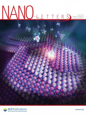
Atomically thin semiconducting oxide on graphene carries a unique combination of wide band gap, high charge carrier mobility, and optical transparency, which can be widely applied for optoelectronics. However, study on the epitaxial formation and properties of oxide monolayer on graphene remains unexplored due to hydrophobic graphene surface and limits of conventional bulk deposition technique. Here, we report atomic scale study of heteroepitaxial growth and relationship of a single-atom-thick ZnO layer on graphene using atomic layer deposition. We demonstrate atom-by-atom growth of zinc and oxygen at the preferential zigzag edge of a ZnO monolayer on graphene through in situ observation. We experimentally determine that the thinnest ZnO monolayer has a wide band gap (up to 4.0 eV), due to quantum confinement and graphene-like structure, and high optical transparency. This study can lead to a new class of atomically thin two-dimensional heterostructures of semiconducting oxides formed by highly controlled epitaxial growth.
Our research focuses on atomic-scale characterization, design, and synthesis as well as the properties of advanced materials including 2D materials, carbon materials, and soft matter by means of aberration-corrected transmission electron microscopy and spectroscopy. In situ experiments at both the atomic and nano scales are implemented for our study.
Advanced TEM Characterization